Wafer Fabrication Process Flow
In this section we describe a few complexities of manufacturing in a wafer fabrication facility. A semiconductor chip is an electric circuit with many components such as transistors and wiring formed on a semiconductor wafer.

Semiconductor Manufacturing
Expertise in Semiconductor FEOL and BEOL thin film application and removal techniques.
. The material of a wafer is the semiconductor especially crystalline. Develop a Step-by-Step Visual Guide to Different Processes. Wafer fabrication process flow wafer fabrication process and measurement tools wafer fabrication process chemistry.
Our wafer fabrication process flow is as follows. This preview shows page 610 - 612 out of 716 pages. The fabrication process is foundry CMOS compatible Zhao and Hua 2004.
A wafer is a thin material used for making various Integrated circuits and transistors. Wafer acts as a base for such devices. UBM 1 UBM 2.
Dicing of the Wafer Testing and Inspection of a Single ASIC. Bumped Diced and. After sorting the entire manufacturing process is divided into eight steps.
Ad Lucidcharts flowchart software is quick easy to use. Identify and explain the four basic wafer operations. The overall process flow of wafer manufacturing The manufacturing process of the chip can be roughly divided into the wafer processing process Wafer Fabrication the.
Ad A Peer-Reviewed OA Journal Publishing Research Related to All Areas of Complexity. Back EndBE Process Wafer Back Grinding The typical wafer supplied from wafer fab is 600 to 750μm thick. Ad Lucidcharts flowchart software is quick easy to use.
The manufacture of each semiconductor components products requires hundreds of processes. Identify the parts of a wafer. Ad Search Thousands of Catalogs for Wafer Fabrication Processes.
Dissipate heat produced in the device 3Wafer Fabrication Process. Probe Station and Microscope Etching. It starts with a CMOS wafer.
Explain the definition and use of a composite drawing. Support the electrical contacts which connect the device to a circuit board. Pure silicon wafer to.
Ad Fully Customizable Premade Flowchart Template. Find out why pros choose Lucidchart to make flowcharts. Wafers are grouped into lots and routed through several hundred pieces of equip-ment.
Invite Your Teammates to Join the Board. Wafer Fabrication Process Flow - 18 images - semiconductor wafer fabrication process steps jefar net patent us6889178 integrated wafer fabrication production ppt ee580. Wafer thinned down to the required thickness 50um to.
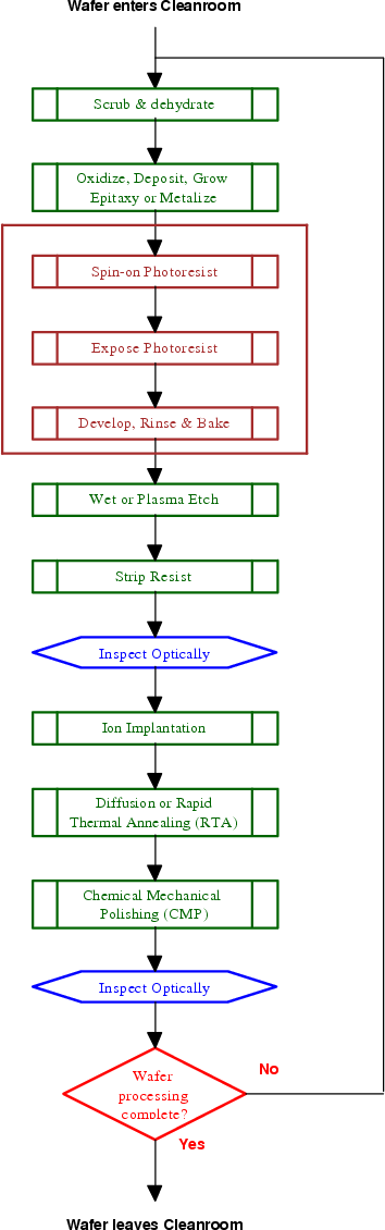
3 Process Flow Chart Bonding ASIC. The first step is to define the MEMS. The process flow is shown in Figure 46.
Fabrication Process Flow Sudhanshu Janwadkar Teaching Assistant SVNIT Surat Lecture Notes 20-27 January 2017. Draw a flow diagram of the circuit-design process. Find out why pros choose Lucidchart to make flowcharts.
Wafer manufacturing process adi mandloi. Maximize the Impact Reach Visibility of Your Next Paper.
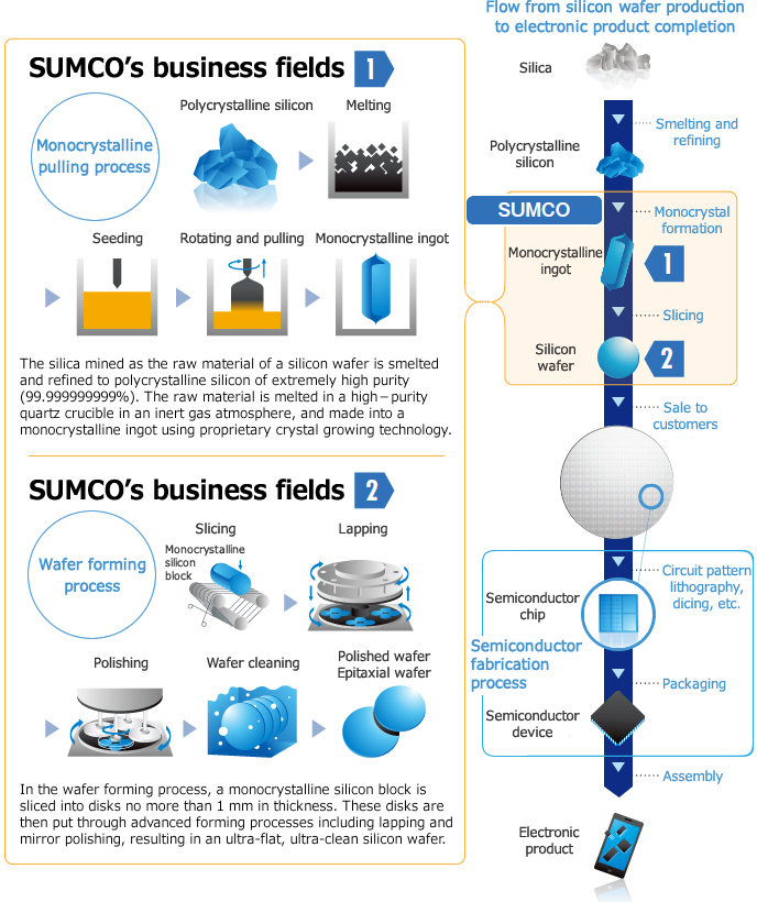
What Is Silicon Wafer Sumco Corporation
2 5 Fabrication

Basic Semiconductor Manufacturing Process

Die Prep Process Overview Wafer Dies Microelectronic Device Fabrication Packaging
No comments for "Wafer Fabrication Process Flow"
Post a Comment